|
|
| (70 intermediate revisions by 4 users not shown) |
| Line 1: |
Line 1: |
| − | This page contains the progress of the fabrication of the Tagger Microscope prototype. Now this is the first Wiki page that I have ever made so please excuse any errors, they will be corrected in a timely fashion. This page will be updated as the project progresses. To see what I am currently working on see [[Weekly Goals]].
| + | The '''tagger microscope''' is a movable, high-resolution [http://en.wikipedia.org/wiki/Hodoscope hodoscope] that counts post- bremsstrahlung electrons corresponding to the photon energy band of interest to the [http://www.gluex.org/ GlueX] experiment in [http://www.jlab.org/Hall-D/ Hall D] at [http://www.jlab.org Jefferson Lab]. While designed as a general-use device, it has been optimized primarily for use in the GlueX experiment, covering the E<sub>γ</sub> range of 8.4-9 GeV (E<sub>e</sub> 3-3.6 GeV) |
| | | | |
| − | == Tools ==
| + | Construction of the tagger microscope prototype is now complete. Below are topics concerning the branches of the work required for its completion and testing in preparation for the construction of the fully-instrumented tagger for Hall D in Jefferson Lab. |
| | | | |
| − | [[Image:workstandassembled.jpg|thumb|Work Stand Apparatus]]
| |
| | | | |
| − | * We designed our own apparatus to cut, polish, and glue the scintillators and the waveguides. For more information on how it works, see [[Work Stand Assembly]].
| + | == R&D Branches == |
| − | * To cut the fibers I use a standard hobby knife.
| |
| − | * For cleaning and polishing acrylic fibers, the recommended tool to use is a plastic nail buff.
| |
| − | * A digital scale (accurate to ±0.01 grams) is used to weigh out the proper proportions of the resin and catalyst.
| |
| − | * Standard laboratory glassware is used for weighing, mixing, and applying the epoxy.
| |
| − | * A laboratory hotplate is used to heat-cure the epoxy.
| |
| − | * An infrared thermometer is used for calibrating the hotplate temperature controls.
| |
| | | | |
| − | For more information (such as prices and product numbers) on the equipment listed above see [[Supplies]]
| + | === R&D into Fiber-Array Fabrication Techniques === |
| | + | :''Main articles: [[Fiber Array Fabrication Techniques]]'' and ''[[Fiber Array Prototype and Mass Production]]'' |
| | | | |
| − | == Fiber Research ==
| + | [[Image:TaggerFocalPlane_ChannelPlan.png|thumb|555px|Scintillating fiber channels as seen by an on-coming electron. Since only energy tagging is required, the members of the 5-channel columns are summed to produce one signal corresponding to that energy channel. The exceptional columns are marked in red - the signals from their individual fibers will be read out to ascertain focal plane orientation and vertical spread. Note the segmentation of the 100-energy bin (column) array into 20 fiber modules. This is thought to be a more manageable design, corresponding nicely to the photo-sensor/electronics grouping.]] |
| | | | |
| − | === Epoxies ===
| + | The design concept for the tagger microscope calls for a scintillating fiber detector array along the focal plane of the spectrally-analyzed beam of electrons. This is a ''two-dimensional'' array broken up into 2 mm<sup>2</sup> patches (as shown in the adjacent figure) representing the cross-sections of the square scintillating fibers. The choice cross-section of the channels is driven largely by considerations of rate. Sensitivity in the vertical direction provided by this two-dimensional array allows for a boost in tagging efficiency (matching electron angular acceptance to that of the photons they produced, which undergo collimation.) |
| | + | To avoid placing photo-sensors along the path of the electronics, the scintillation light will be delivered to separately-mounted sensors and electronics via clear fiber waveguides. |
| | | | |
| − | The two epoxies that are being tested are:
| + | Development of fiber cutting, polishing and gluing techniques to enable the most efficient capture and delivery of scintillation light is being conducted by Brendan Pratt and James McIntyre |
| − | * BC-600 (Bicron) [http://www.detectors.saint-gobain.com/media/documents/S0000000000000001004/SGC%20BC600%20Data%20Sheet%200105.pdf/ BC-600 Info]
| |
| | | | |
| − | * 20-3238 (Epoxies Etc) [http://www.epoxies.com/tech/20-3238R.pdf/ 20-3238 Info]
| + | === Scintillation Detection Sensors === |
| | | | |
| − | === Cleaving and Polishing Techniques ===
| + | [[Image:SSPM06_(2x2).jpg|thumb|113px|4.4 mm<sup>2</sup> active area Silicon Photomultiplier]] |
| − | <u>Note:</u> This process assumes that the uncut scintillators and waveguides are in segments or spools of more then 3 meters long. Please read each step completely before you begin this process. | |
| | | | |
| − | '''Step 1: Cleaving''' | + | :''Main article: [[Characterizing SiPMs]]'' |
| − | * Technique 1
| |
| − | ** Place the fiber in the apparatus as shown in ''Work Stand Assembly'' under ''Cleaving''. Take the hobby knife and place it on the fiber (again look under ''Work Stand Assembly'' for the proper placement of the blade) and gently tap the butt end of the knife until the fiber is cut cleanly. Remove the fiber and inspect the freshly cleaved end. Look for any major breaks in the outer cladding (use magnifying glass if necessary). I will be posting pictures (as they become available) as to what is acceptable and unacceptable breaking in the cladding.
| |
| − | ** If the ends of the cleaved scintillators have major breaks in the outer cladding, then the best course of action it to toss out the unusable segment, properly polish the end attached to the spool and repeat Step 1. If the ends of the cleaved scintillators are border line acceptable proceed to Step 2.
| |
| − | ** For the waveguides, it is best to give yourself an extra 1/2 cm of fiber in case the cleaved end has major breaks in the outer cladding.
| |
| | | | |
| − | * Technique 2
| + | A search for a solid state photo-sensor satisfying the tagger requirements has been conducted. The new Silicon Photomultipliers (SiPMs) are thought to fit this application better than the traditional Photo-Multiplier Tubes (PMTs) due to the nice properties of the former, including match of fiber cross section, low bias voltage and other factors. See the main page of this project for this design choice justification as well as detailed performance analysis of tested SiPMs produced by [[User:Senderovich|Igor Senderovich]] and Richard Jones. |
| − | ** If you want to ensure that the outer cladding will not be disturbed during the polishing process you will need to remove the outer cladding for a short (about 0.5 mm) length of the fiber. This is a relatively easy process it just takes some time a lot of patients, and a microscope. To begin with, set up a cutting guide such that you can make a small cut perpendicular to the length of the fiber. If possible try and design your cutting guide such that it also lines up the cuts for all of the sides. I used a simple piece of paper raped around the fiber.
| |
| − | ** Next, using your hobby knife make a shallow cut along your cutting guide.(Note: you don't have to cut all the way through the outer cladding, just most of the way.) Try not to cut the inner fiber, to insure that you do not, it takes some practice. Take a piece of scrap fiber and begin cutting the outer cladding. The inner fiber feels much softer then the outer cladding, the only way to tell is it just cut through your test fiber. [[Image:Stripped Cladding.JPG|thumb|Fiber with Cladding Striped]]
| |
| − | ** Now that each side of the fiber is cut, start removing the cladding. To do this, it is easiest to use a second hobby knife. Place the second hobby knife along the cut in the fiber and place the initial hobby knife at the end of the fiber between the cladding and the fiber and use it to pry up the cladding. If you did it right the cladding should come up and break along the cut that you made. The fiber after the cladding is removed, is see in the picture to the right. (Note: don't worry about scratching the inner fiber, it will all be polished away anyway.)
| |
| − | ** Finally, during polishing, make sure to shave the fiber almost all the way down to the cladding.
| |
| | | | |
| − | '''Step 2'''
| |
| − | * <u>Scintillators:</u> The segments cut using the ''Work Stand Assembly'' have an extra millimeter or so in length made by design so that by the end of the polishing process the segment will be of the proper length of 2 cm. That being said, if the fiber is border line unacceptable, see if the cladding is broken too far as not to be recovered by polishing.
| |
| | | | |
| − | * <u>Waveguides:</u> With that extra 1/2 cm you alloted yourself, it should be possible to recover, through polishing, most if not all the unacceptable fibers.
| + | === Photo-Sensor Support Electronics === |
| | | | |
| − | '''Step 3: Polishing''' | + | :''Main article: [[Design and prototyping of SiPM electronics]]'' |
| − | * Arrange the fiber in the apparatus as shown in ''Work Stand Assembly'' under ''Polishing''. If the end to be polished is significantly longer then the desired length (i.e. 0.2 cm or more), begin with the coarse emery board . If total length is less than 0.2 cm of desired length, begin with the much less coarse nail buffs (pictures of the nail buffs will be posted).
| |
| − | **<u>Note:</u> It seems that the color of the nail buffs signifies how fine or coarse the buff is. So if you cannot find the exact nail buffs that I used, just try to match the color of each and you should be fine.
| |
| | | | |
| − | * Using the emery board is a bit tricky and needs special care. Gently grind down the end of the fiber with the board, do not push too hard or to soft. The strokes should be at a steady pace but not too fast or to slow (if you consider the up and down motion as one complete cycle the speed should be around 1 revolution per second). I know that these direction are a little obscure, so the best way to figure out just how fast and how much pressure to apply is to use a scrap fiber and practice for yourself. The reason why you do not want to go too fast or apply too much pressure is that it could (and most likely will) result in stripping the outer cladding around the fiber. After the fiber is polished down with the emery board, it is best to remove it from the apparatus and inspect it for major breaks in the outer cladding. This process should take about 30 seconds depending on how much you need to shave off.
| + | A project pertaining to design and prototyping of electronics pertaining to bias, amplification and control of the photo-sensors described above has been conducted by Brendan Krueger, [[User:Senderovich|Igor Senderovich]], and Woody Underwood. Due to the expected variability of performance of these solid-state sensors as well as variation in optical efficiency among the channels, the electronics has been designed to provide individually selectable bias voltage, controlled amplification over a wide range of light intensities, as well as feedback on "board health": state of key voltages and temperature readings at various points. Additionally, the summation of signals over scintillator channels vertical in the focal plane is incorporated. Communication with the tagger electronics for monitoring and bias control will be done of Ethernet. |
| | | | |
| − | * Use the nail buffs on the fiber in the order of Black, White, Gray (I used 3 different ones because they came in a set, but if you just use the first (black) and last(gray) i think you should be fine). With these you do not have to be as cautious as you did with the emery boards but still some care needs to be taken. Basically follow the same process as for the emery board. When you feel, through the buff, the fiber become smooth, it is time to switch to the next buff. Be sure not to over polish the fiber or round off the ends. If the ends are rounded, the epoxy will not adhere properly to the fiber.
| |
| | | | |
| − | * Here are pictures of what the fiber should look like after each step [[Fiber Pictures]]
| + | === Mechanical Design of the Tagger Microscope === |
| | | | |
| − | == Gluing ==
| + | :''Main article: [[Tagger Microscope Mechanical Design]]'' ([[User:Senderovich|Igor Senderovich]], [[User:mcintyre|James McIntyre]]) |
| − | The gluing process is on going, so there will be updates to this section.
| |
| | | | |
| − | * <u>Setup:</u>
| + | Mechanical design of the full-scale tagger microscope is well underway. The design is intended to simplify the repetitive components necessary while maximizing the flexibility of the device. In particular, the drastic dependence of the electron crossing angle with energy has been taken account: the device will have the ability for orientation of its fiber modules to match any segment in the useful energy range. |
| − | ** There is quite a bit to set up before you begin actually applying epoxy. To start, make sure you have the following supplies:
| + | Additionally a movable internal pulser for testing and a three-point remote-control-adjustable plane for the fiber array are under design. |
| − | *** Lab Gloves
| |
| − | *** Kim wipes
| |
| − | *** Digital scale
| |
| − | *** Acetone and Isopropanol
| |
| − | *** A container to mix the epoxy, and a waist container
| |
| − | *** The resin and catalyst (or hardener) of the epoxy
| |
| − | *** A pipette with tip and dispensing pump
| |
| − | *** Tongue depressors
| |
| − | ** Once you have collected all the necessary equipment you can begin setting up for gluing. First and foremost, PUT ON GLOVES. Now, take out several kim wipes and place them under the digital scale, the waist container, the resin and catalyst, and on anything that could have unwanted chemicals spilled on. Set 3 or 4 tongue depressors, and 3 or 4 pipettes, off to the side of your workstation so that they are not in the way but easily accessible. Pour some Acetone or Isopropanol in your waist container for quick cleaning. Inspect all glassware make sure that they are completely clean. If you find glassware that is not clean, clean it using Acetone and then wait at least 10 minutes before using the glassware. Now that you are all set up you can begin gluing.
| |
| | | | |
| − | Here is a picture of all the new equipment that is required for the new application process.
| |
| | | | |
| − | [[Image:Pipette equip.JPG|thumb|center|Pipette equipment]]
| |
| | | | |
| − | * <u>Epoxy 20-3238</u>
| + | == Beam Test in Hall B at Jefferson Lab == |
| − | ** Weigh out your resin and catalyst, this is a MAJOR factor in the success of the experiment so take your time in mixing and getting the exact amounts of resin and catalyst (100 parts resin to 30 parts catalyst).
| + | |
| − | ** Once you have the two components weighted out, mix them together. The mixture should turn mildly opaque and become viscus. When the components are mixed completely, the mixture should turn clear and the viscosity should thin out a bit (becoming more like cooking oil in viscosity).
| + | The ideal place to test the prototype is near another tagger magnet such as the one in Hall B. Thus the plan is to set the prototype downstream of Hall B's hodoscope. |
| − | ** There will be bubbles left in the mixture. To get rid of them, just let sit for about 10 or 15 minutes, for the bubbles to come to the surface. Then gently pop the bubbles with a tongue depressor. Now since the pot life of epoxy is 40 to 45 minutes, you will have plenty of time to get rid of the bubbles. [[Image:Setup Noepoxy.JPG|thumb|Fibers Setup Before Epoxy]]
| + | |
| − | ** Once you have the mixed the epoxy, lay the fibers out in the apparatus how you want them to be glued together like in the picture seen to the left, click on the picture to get a better look at the fibers. Make sure that the ends of the fibers are clean and polished before applying the epoxy. (Note: This can and should be done while you wait for the bubbles to escape from the epoxy. Also picture taken under microscope.)
| + | * [http://zeus.phys.uconn.edu/~senderovich/GlueX/Tagger/Reports/MicroscopeBeamTest_plan-2-2010/MicroscopeBeamTest_plan-2-2010.pdf Beam Test Plan] |
| − | ** Now that you have the fibers set and ready to receive the epoxy, Take a clean pipette with a dispensing pump and apply a tip to the end of the pipette. (Note: It was not extremely easy to tell when a tip is completely attached to the end of the pipette, so practice before attempting this would be best.) [[Image:Glued Fibers.JPG|thumb|left|Fibers After Epoxy]] | + | * [[Delivery of the Tagger Microscope Prototype to JLab]] - [[User: mcintyre|James McIntyre]] |
| − | ** With the tip on the pipette, get a small amount of the epoxy in the pipette, and then apply to the small gap between the two fibers. The final result should look like the picture seen to the right. Again click on the photo to see a bigger image. | + | * [https://docs.google.com/document/pub?id=1yC9U8ufcUvTR00vY2vNM_G78fwLKALBip3E1Zsic1R4&embedded=true Spring 2011 Beam Test of Tagger Microscope Prototype] - online logbook |
| − | ** Now that the epoxy has been applied, make the final adjustments to the fibers to make sure that they are at the distance desired and that they are lined up properly. (All the adjustments should be minor ones resulting from the application process) Then let the epoxy cure for 18 to 24 hours at STP, or for 1 to 2 hours at 60 Celsius. | + | |
| | + | |
| | + | == References == |
| | + | * [[Microscope Prototype Mechanical Design Drawings]] - [[User: mcintyre|James McIntyre]] |
The tagger microscope is a movable, high-resolution hodoscope that counts post- bremsstrahlung electrons corresponding to the photon energy band of interest to the GlueX experiment in Hall D at Jefferson Lab. While designed as a general-use device, it has been optimized primarily for use in the GlueX experiment, covering the Eγ range of 8.4-9 GeV (Ee 3-3.6 GeV)
Construction of the tagger microscope prototype is now complete. Below are topics concerning the branches of the work required for its completion and testing in preparation for the construction of the fully-instrumented tagger for Hall D in Jefferson Lab.
R&D Branches
R&D into Fiber-Array Fabrication Techniques
- Main articles: Fiber Array Fabrication Techniques and Fiber Array Prototype and Mass Production

Scintillating fiber channels as seen by an on-coming electron. Since only energy tagging is required, the members of the 5-channel columns are summed to produce one signal corresponding to that energy channel. The exceptional columns are marked in red - the signals from their individual fibers will be read out to ascertain focal plane orientation and vertical spread. Note the segmentation of the 100-energy bin (column) array into 20 fiber modules. This is thought to be a more manageable design, corresponding nicely to the photo-sensor/electronics grouping.
The design concept for the tagger microscope calls for a scintillating fiber detector array along the focal plane of the spectrally-analyzed beam of electrons. This is a two-dimensional array broken up into 2 mm2 patches (as shown in the adjacent figure) representing the cross-sections of the square scintillating fibers. The choice cross-section of the channels is driven largely by considerations of rate. Sensitivity in the vertical direction provided by this two-dimensional array allows for a boost in tagging efficiency (matching electron angular acceptance to that of the photons they produced, which undergo collimation.)
To avoid placing photo-sensors along the path of the electronics, the scintillation light will be delivered to separately-mounted sensors and electronics via clear fiber waveguides.
Development of fiber cutting, polishing and gluing techniques to enable the most efficient capture and delivery of scintillation light is being conducted by Brendan Pratt and James McIntyre
Scintillation Detection Sensors
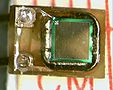
4.4 mm
2 active area Silicon Photomultiplier
- Main article: Characterizing SiPMs
A search for a solid state photo-sensor satisfying the tagger requirements has been conducted. The new Silicon Photomultipliers (SiPMs) are thought to fit this application better than the traditional Photo-Multiplier Tubes (PMTs) due to the nice properties of the former, including match of fiber cross section, low bias voltage and other factors. See the main page of this project for this design choice justification as well as detailed performance analysis of tested SiPMs produced by Igor Senderovich and Richard Jones.
Photo-Sensor Support Electronics
- Main article: Design and prototyping of SiPM electronics
A project pertaining to design and prototyping of electronics pertaining to bias, amplification and control of the photo-sensors described above has been conducted by Brendan Krueger, Igor Senderovich, and Woody Underwood. Due to the expected variability of performance of these solid-state sensors as well as variation in optical efficiency among the channels, the electronics has been designed to provide individually selectable bias voltage, controlled amplification over a wide range of light intensities, as well as feedback on "board health": state of key voltages and temperature readings at various points. Additionally, the summation of signals over scintillator channels vertical in the focal plane is incorporated. Communication with the tagger electronics for monitoring and bias control will be done of Ethernet.
Mechanical Design of the Tagger Microscope
- Main article: Tagger Microscope Mechanical Design (Igor Senderovich, James McIntyre)
Mechanical design of the full-scale tagger microscope is well underway. The design is intended to simplify the repetitive components necessary while maximizing the flexibility of the device. In particular, the drastic dependence of the electron crossing angle with energy has been taken account: the device will have the ability for orientation of its fiber modules to match any segment in the useful energy range.
Additionally a movable internal pulser for testing and a three-point remote-control-adjustable plane for the fiber array are under design.
Beam Test in Hall B at Jefferson Lab
The ideal place to test the prototype is near another tagger magnet such as the one in Hall B. Thus the plan is to set the prototype downstream of Hall B's hodoscope.
References
.jpg)