Programming the temperature sensor
Interface
The AD7314 temperature sensor uses a four-wire interface related to (and compatible with) the SPI bus protocol. The wires are:
- CE: Chip Enable (input), positive logic enable for SCLK
- SCLK: Serial Clock (input), clock line supplied by external source
- SDI: Serial Data In (input), data input line
- SDO: Serial Data Out (output), data output line
Note that the input/output notations are for slave devices (such as the temperature sensor) but are reversed for master devices (such as the FPGA). Proper SPI protocol flips the I/O polarity of CE and SCLK and crosses the SDI and SDO lines so that SDI is an input on every device and SDO is always an output. To maintain simplicity in wiring conventions we are not using proper SPI protocol, but are calling the slave input/master output line SDI and the slave output/master input line SDO so that the SDI/O notations are proper for slaves. The maximum clock rate is no higher than 10MHz. The interface, having separate input and output lines, is full-duplex; in fact the temperature sensor is unable to function in half-duplex mode. Outputs from the temperature sensor change on rising edges of SCLK, but inputs are latched on falling edges.
There is only one write operation to the temperature sensor and that is used to direct the temperature sensor to enter power-down mode. We do not plan to use this mode, so the SDI input on the temperature sensor will be tied to ground.
A read operation occurs during a 16-cycle pulse of CE. The first transmitted bit will be zero, followed by ten bits of temperature data (MSB first). The remaining five bits are copies of the final data bit. After CE goes low SDO goes into a high-Z state. Temperature data is given in degrees Celsius. The format is two's-complement with two decimal places; in essence it is standard two's-complement, then the result must be divide by four after converting to decimal.
Emulator
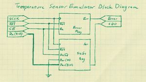
The functional block diagram for the emulator is shown to the right. The blocks are:
- Error Flag
- The error flag goes high if the enable line is high for 1-15 or 17+ cycles. It resets to low any time the enable line goes back to high. It is used to notify of a "bad" transmission (not 16 cycles long).
- inputs
- Clk: clock
- Rst: asynchronous, active-low reset
- En: enable
- outputs
- Err: error flag
- Shift Reg
- An 11-bit, parallel-in, serial-out shift register that loads when not shifting.
- inputs
- Clk: clock
- Rst: asynchronous, active-low reset
- Sh/Ld: active-high shift, active-low load
- Par(10:0): 11-bit parallel input bus
- outputs
- Ser: serial output line
Controller
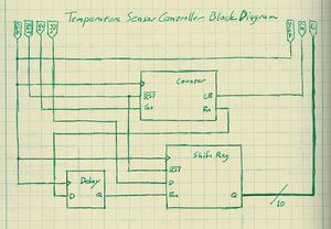
The functional block diagram for the controller is shown to the right. The blocks are:
- Counter
- Counts a cycle of 17 pulses; holds En high for 11 pulses, holds CE high for 16 pulses.
- inputs
- Clk: clock
- Rst: asynchronous, active-low rest
- Go: trigger to begin cycle
- outputs
- CE: serial chip enable
- En: internal shift enable
- Delay
- Delays input by one clock cycle.
- inputs
- Clk: clock
- D: input signal
- outputs
- Q: output signal
- Shift Reg
- A 10-bit, serial-in, parallel-out shift register.
- inputs
- Clk: clock
- Rst: asynchronous, active-low rest
- D: input signal
- En: shift enable
- outputs
- Q: 10-bit output bus

