FPGA Programmer
(110) DAC Programmer
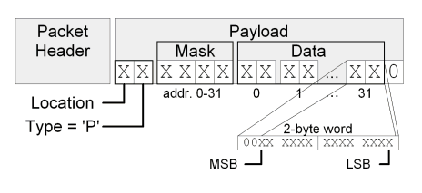
The DAC Programmer assigns DAC voltages according to the mask and values listed in the P-packet payload. The module always passes control to the Transmitter to send a D-packet, confirming the requested values.
The mask selects which channels must be altered. Any channel that is to be reprogrammed will have a 1 in the corresponding location, and any channel that is to be left alone will have a 0 in the corresponding location. The MSB of the first byte will be channel 0 and the LSB of the fourth byte will be channel 31. Thus, if only channels 5 through 17 are to be programmed, the mask would contain:
| First data byte | 0 | 0 | 0 | 0 | 0 | 1 | 1 | 1 |
|---|---|---|---|---|---|---|---|---|
| Second data byte | 1 | 1 | 1 | 1 | 1 | 1 | 1 | 1 |
| Third data byte | 1 | 1 | 0 | 0 | 0 | 0 | 0 | 0 |
| Fourth data byte | 0 | 0 | 0 | 0 | 0 | 0 | 0 | 0 |
Programming Details
The Programmer is one of the more complex modules. There are two stages involved in its process: mask and data. The first stage involves reading and storing the 4-byte mask (32-bits corresponding to 32 channels of the DAC), which follows immediately after the location and type bytes of the P-packet payload. Then the Programmer steps through the rest of the P-packet in 2-byte words, each containing the 14-bit DAC voltage, ordering write operations via the DAC Controller for each one. The packet is expected to have all 32 values in ascending order of channels. For any channels that need not be altered the mask must contain 0's for the corresponding bits. If a requested value exceeds the voltage level hardwired into the FPGA firmware, this maximum value is set instead of that requested by in the P-packet. The responding D-packet will reflect this correction.
The DAC Register is pulsed simultaneously with the DAC controller to record the programmed value. These will later be sent back to the PC for confirmation. (No feedback from the DAC chip itself is possible. Channel 31 is reserved for calibration and is connected to ADC channel 7.) Because the combined duration of these operations exceeds the reception time of the minimum-length packet, the module inhibits the Receiver Interface of the Ethernet Controller for the duration of the programming to prevent incoming packet pileup and receive buffer overload.
Ports
- Clk: [in] clock
- Rst: [in] asynchronous reset
Write signals to the DAC Controller and DAC Register
- DAC_iGo: [out] active-low "Go" signal
- DACReg_En: Enable (write) signal to DAC Register
- DAC_Addr: [out] 5-bit DAC channel address
- DAC_D: [out] 14-bit voltage value for the register and DAC Controller
- DAC_Done: [in] "Done programming" signal from DAC controller
State Register Control Lines
- state_En: [out] state register enable (write) signal
- state_D: [out] (3-bit) state register input
- state_Q: [in] (3-bit) state register output
Transceiver Control Lines
- TxRx_Go: [out] "Go" signal to read/write an EC control register byte
- TxRx_RiW: [out] active-high read, active-low write flag
- TxRx_Aout: [out] EC control register address (8-bit)
- TxRx_Din: [in] EC control register return value
- TxRx_Dout: [out] EC control register write value
- TxRx_Done: [in] "Done" signal from Transceiver
