Ethernet packets
This page details the packets we will send across our internal network to define the standards of communication between the digital boards and the controlling PC. Both the FPGA designer and the PC software programmer will need to make reference to this page in order to coordinate their respective designs.
Structure of a packet
Transmitting
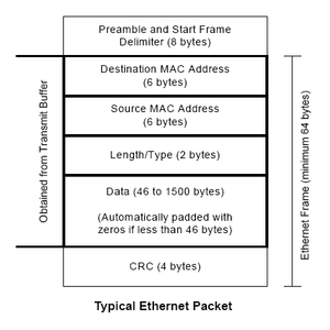
To the right is a diagram depicting the structure of an Ethernet packet. On the left side is marked the blocks that must be defined by the FPGA to be passed to the CP2200/1. The first 8 bytes ("Preamble and Start Frame Delimiter") and last 4 bytes ("CRC") will be generated by the CP2200/1, so the FPGA need not even be aware of them. The first significant block is the 6-byte destination MAC address. The FPGA will have to store this to know the address of its conversation partnet. The next block is the 6-byte source MAC address. Each CP2200/1 comes with a factory-set unique MAC address stored in the last page of Flash memory that will be used as the source MAC address. This address must be retrieved at startup, insterted in the MAC interface of the CP2200/1 as well as stored by the FPGA for packet addressing. The next block is the 2-byte length block. This is the number of bytes of data, i.e. everything between the length block and the CRC. Then finally comes the data block, which must be padded to a minimum of 46 bytes but cannot exceed 1,500 bytes. In practice, out packets are padded to 47 bytes of payload: the letter of the CP2200/1 manual seems to indicate although this is likely a mistake. (Their likely error reduces to the fact that N-member array with first index 0 ends with index N-1, not N.)
Receiving
The CP2200/1 appears to give access to the entire 64-byte (minimum) packet, which would include everything on the above diagram except for the "Preamble and Start Frame Delimiter". The CP2200/1 can be programmed to filter out any packets not addressed to it, but it only verifies the first 5 bytes of the MAC address, which is useless, given that out system would likely be equipped with a single batch of controllers, differing only in the last octet of their MAC address. For good packets the FPGA can strip away and ignore the first 14 bytes (it does not need the length field, as we define our own standard for the packets below, using the first two data bytes to specify intended physical address and packet type.) From there the FPGA can parse the data field according to the specifications outlined below.
Packets from the PC to the FPGA
We will use six types of packets in our communications, paired into three "conversations" or "cycles": a reset cycle, a query cycle, a programming cycle. Each packet's data section will begin with a single-byte code to identify the packet type. As a mnemonic, these bytes will use ASCII codes to represent a single-letter shorthand for each packet.
The reset cycle - "R" packets
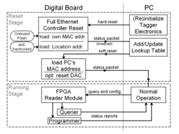
The reset cycle is a conversation whose purpose is to reset the digital control board. On each power-on, the various chips on the digital board need to be re-initialized. This includes the Ethernet chip itself, so the reset functionality needs to be built into the FPGA logic by default and needs to execute on start-up with no external stimulus in order to obtain Ethernet control. However it may also be necessary to instigate a reset externally for some reason. This cycle allows the external PC to initiate a reset and will notify the PC when the system is fully initialized.
Additionally, the reset cycle gives the tagger boards and PC a chance to build the proper address maps. The boards acquire the MAC address of the PC and the PC builds a MAC-Location table, where the "Location" is a hard-coded 8-bit slot identifier hard-coded into the bus-board. This organization step is necessary for the PC to be able to pinpoint SiPM channel groups.
The "R group" of packets sent from the PC to the card to initiate a reset process in various forms. Two possible reset packets (corresponding to two degrees of reset) are possible
- Full or "Hard" reset: This resets all chips on the board. This will contain no data as no further instructions can be remembered after a board reset.
- Selective or "Soft" reset: This will have flags to reset the Ethernet chip, the ADC/Temperature sensor group (SPI bus), and the DAC.
R-packet - hard reset
The packet type byte (2nd in packet payload) will be an ASCII R: 0x52, 0101 0010. This packet orders control passed to the Reset_hard module which resets the Ethernet Controller chip (EC) loads its own MAC address and transmits an S-packet to confirm completion of this stage and allow the PC to pair the source MAC address with the included slot Location address (always in the 1st byte of payload).
R'-packet - soft reset
The packet type byte (2nd in packet payload) will be a 0xD2, 1101 0010 - essentially an ASCII R with the MSB flipped to '1'. This packet orders a more customized "soft" reset. After the mandatory Location and Packet Type bytes, this packet carries the 6-byte PC MAC address (to allow the FPGA to record the address of its conversation partnet) as well as a debug byte and a reset mask for the on-board chips. The syntax of the debug byte has not been defined yet, but the reset mask currently the two least significant bits as reset flags for SPI bus (bit 1) and DAC (bit 0). Another S-packet is returned after this stage.
The query cycle - "Q" packet
The query cycle is a conversation regarding the status of the digital board. It polls the sensor devices and reports back their most recent data.
The Q-packet is sent from the PC to the FPGA to request a status report from its sensor chips. Again, there is no relevant data aside from the packet type. There is no data attached to a query packet: the FPGA triggers the query module upon recognizing a Q-type packet, which is identifiedan ASCII Q: 0x51, 0101 0001 in the packet type field (2nd byte of packet payload)
The programming cycle - "P" Packet
The programming cycle is a conversation intended to set the values of the DAC channels. It sends programming data to the board and receives confirmation of the programming.
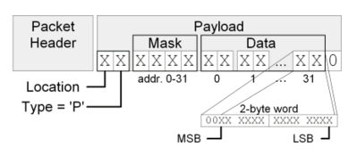
This is the packet sent from the PC to the FPGA to set new values to the DAC channels. The first byte of the packet will be an ASCII P: 0x50, 0101 0000. The next four bytes (if all 32 channels are used; 3 if 24 channels, 2 bytes if 16 channels) together form a programming mask. Any channel that is to be reprogrammed will have a 1 in the corresponding location, and any channel that is to be left alone will have a 0 in the corresponding location. The MSB of the first byte will be channel 31 (or 23 or 15) and the LSB of the fourth (or third or second) byte will be channel 0. Thus, if all 32 channels are to be used, but only channels 14 through 26 are to be programmed, the packet would contain:
| First data byte | 0 | 0 | 0 | 0 | 0 | 1 | 1 | 1 |
|---|---|---|---|---|---|---|---|---|
| Second data byte | 1 | 1 | 1 | 1 | 1 | 1 | 1 | 1 |
| Third data byte | 1 | 1 | 0 | 0 | 0 | 0 | 0 | 0 |
| Fourth data byte | 0 | 0 | 0 | 0 | 0 | 0 | 0 | 0 |
Following this are 64 bytes of programming data listing the values for channels 0-31 (in that order) in 2-byte words. Each channel needs 14 bits, so the format is two leading zeros and 6 MSB of data is the first byte, then 8 LSB of data in the second byte. All channels are present in the packet, but only those marked in the mask will be programmed; all other bytes will be ignored and can take on any value. The total size of the data in a programming packet is:
Packets from the FPGA to the PC
"S" packet: status report
This is the packet sent from the FPGA to the PC to report on the current status of the board. The first two bytes of the packet will be the usual Location-stamp byte and the packet identifier: an ASCII S: 0x53, 0101 0011. After that will come the status data.
- The first two bytes of data will be the temperature. The temperature sensor returns 10 bits of data. The first byte will contain six leading zeros, then the two MSB of data. The second byte will contain the 8 LSB of data.
- The next 16 bytes of data will be the ADC channels. The ADC returns 8 channels of 12 bits each. The first byte for each channel will have four leading zeros, then the 4 MSB of the data. The second byte for each channel will contain the 8 LSB of the data. The channels will be reported from channel zero to channel seven.
This totals 20 bytes: one for Location, one for Packet Type, two of temperature, sixteen of voltages.
"D" packet: DAC setup complete
This is the packet sent from the FPGA to the PC to confirm that the DAC has been programmed to specifications. The first byte of this packet is an ASCII D: 0x44, 0100 0100. The next 64 bytes are the values of the DAC channels. As before, the format is two leading zeros and 6 MSB of data in the first byte and 8 LSB of data in the second byte. The channel values are listed from 0 to 31. This confirms to the PC that the data was programmed according to specification and helps synchronize the control board and the PC. All channels are reported back, not just those that were reprogrammed during this conversation. Note that the DAC chip has no interface for querying the state of particular channels. The values reported are the nominal programmed values simply confirming that the correct values were received. If there remain free ADC channels, they can perhaps be wired to sample some DAC lines in order to have some real confirmation.


