Difference between revisions of "Surface Images and Thickness profile of Diamonds"
Jump to navigation
Jump to search
| Line 6: | Line 6: | ||
---- | ---- | ||
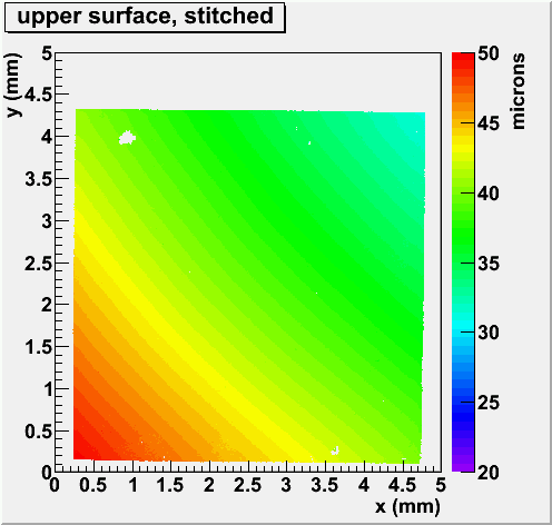
[[File:25_Upper.png]] | [[File:25_Upper.png]] | ||
| + | [[File:25_Lower.png]] | ||
| + | [[File:25_Thick.png]] | ||
== sinmat - 90 == | == sinmat - 90 == | ||
Revision as of 01:58, 20 February 2013
Zygo Images of Diamond Radiators
sinmat - 30
30 micron thick sinmat diamond
 File:25 Lower.png
File:25 Thick.png
sinmat - 90
Got from sinmat as 50 micron but was imaged and found to be 90 microns
Upper surface, Lower surface and thickness profile images
sinmat -150
Got from sinmat as sinmat 100 but was imaged and the thickness was found to be 150 microns thick .
J1a50
50 micron thick diamond from JLAB
J2a50
50 micron thick diamond from JLAB
J2a100
100 Micron thick diamond from JLAB