Pulser amplitude feedback amplifier
Purpose
The pulse generator built by Alex Barnes and Jon Kulakofsky produces -10V pulses of duration 1ns fwhm. These pulses are split 90:10 at the output of the pulse generator circuit, and driven out two coaxial cables. The -1V signal matches expectations for a NIM logic signal, and is fed into a discriminator to generate a trigger for the data acquisition. The coaxial cable carrying the -9V pulse is coupled directly from the coax cable conductors to the pins of a laser diode of type DL3148-025 - 635 nm, 5 mW, Ø5.6 mm. The specs for the laser diode are shown at the bottom of this page. The data sheet for the laser diode shows the pin-out for the round 5.6mm package. Pin 2, which is internally shorted to the brass device enclosure, is tied to the braid on the coax, while the coax core conductor is tied to pin 1. Negative pulses provide a forward-biased signal to drive the diode laser. The third pin of the chip is connected to an internal photodiode. If the photodiode is reverse-biased, it generates a current proportional to the intensity of the light in the laser cavity. The photodiode current is said to be 200uA at full laser intensity. It has a stated maximum reverse bias of 30V, but one would guess that it is fully depleted with a reverse bias of only 2-3V. The current from a 1ns pulse would be 200fC. Stretching 200fC over 40ns to have a sufficient pulse width for accurate digitization leaves a pulse maximum of 5uA = 0.25mV at the adc input. Amplification is required if this signal is to be used for pulse height normalization.
Circuit diagram and layout
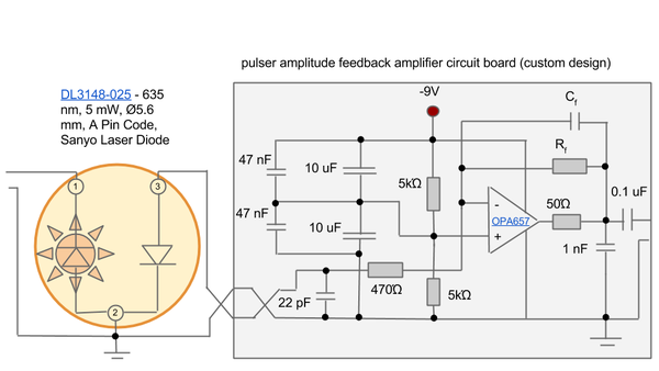
The final design is shown in the figures below. It went through considerable evolution during the prototyping phase because we had trouble with high-frequency oscillations of the op-amp. The phase shift between the inputs and the output goes through 180 degrees around 1GHz, but the exact frequency where that occurs turns out to depend a lot on how the output is loaded. The 180 degree point is where instability occurs because at that point feedback to the inverting pin essentially becomes positive feedback. With the following measures, we were eventually able to suppress the oscillations.
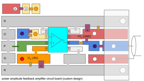
- Combine multiple strips around the op-amp region on the circuit board to play the role of a low-inductance ground plane.
- Put a pair of bypass capacitors (10uF, 47nF) between the power pins of the op-amp and the low-inductance ground plane. Locate the 47nF capacitor as close as possible to the power pin on the chip.
- Limit the current on the output pin by putting a 47 Ohm resistor in series with all loads, even the feedback path which might have a ~1 pF of capacitance to ground.
The last step proved to be crucial. The manufacturer's data sheet warns about instability if the output pin is not protected by a resistor, and even gives a table of recommended resistance values depending on the capacitance of the output net to ground. At first I resisted this because it means giving up output amplitude, but it turned out to be the key step needed to achieve stability.
Figure 1. Circuit diagram of the pulser amplitude feedback amplifier, showing external connections to the 9V power supply, the laser diode package, and the output signal which generates the amplitude feedback pulses.
Figure 2. Layout of the pulser amplitude feedback amplifier circuit board, showing external connections to the 9V power supply, the laser diode package, and the output signal which generates the amplitude feedback pulses. The layout is designed for a standard prototype PCB with traces running in one direction across the board and holes on a 1/10 inch grid. The 9V battery is mounted on the back side of the board. External wires to the laser diode are labeled as 2 and 3. Capacitors are colored purple, resistors are light brown, and wired connections are gray or green. Filled circles represent wired connections on the back side of the board, with the fill color indicating the matched pairs.
| 500px | 500px |
Figure 3. Photograph of the component side (left panel) and back side (right panel) of the feedback amplifier circuit board.
Output pulses
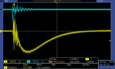
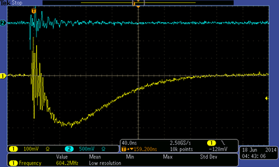
Below are some traces of output pulses from the pulser amplitude feedback amplifier, taken with the 350MHz oscilloscope and with the 250MHz FADC (analog bandwidth 100MHz).
| 
|
Figure 4. Oscilloscope traces of pulses from the pulser amplitude feedback circuit, showing several pulses superimposed (left panel) and a single pulse (right panel). The upper trace (blue) is the NIM trigger signal from the pulse generator. The lower trace (yellow) is the photodiode signal, as shaped and amplified by the feedback circuit. The high frequency oscillations at the beginning of the photodiode pulse are the result of pickup from the large instantaneous pulse currents flowing on the laser diode pins during the intense 1ns pulse. The amplifier stretched the feedback pulse so that it reaches a maximum after these transients have died away.
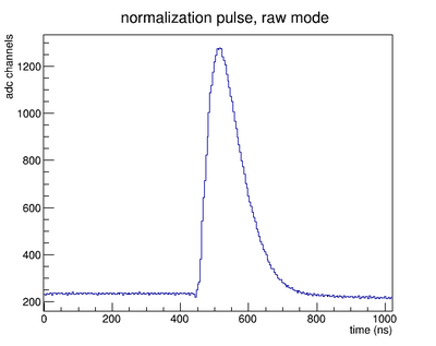
Figure 5. Raw data recorded by the FADC250 on the pulser amplitude feedback channel. Pulse-to-pulse shape variation is very slight apart from overall magnitude fluctuations, which are at the level of 1%.
