Difference between revisions of "Pulser amplitude feedback amplifier"
| Line 9: | Line 9: | ||
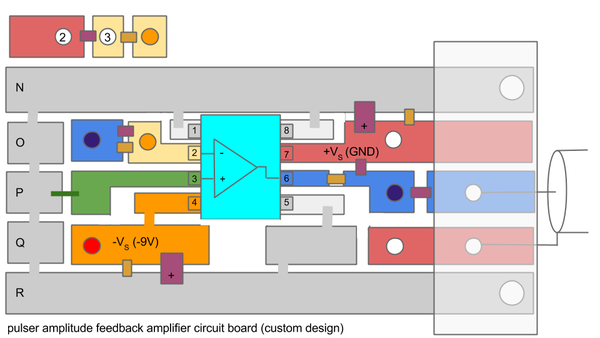
[[image:laserDiode_pd_amp(2).png|600px|center]] | [[image:laserDiode_pd_amp(2).png|600px|center]] | ||
| + | <blockquote> | ||
| + | Figure 2. Layout of the pulser amplitude feedback amplifier circuit board, showing external connections to the 9V power supply, the laser diode package, and the output signal which generates the amplitude feedback pulses. The layout is designed for a standard prototype PCB with traces running in one direction across the board and holes on a 1/10 inch grid. The 9V battery is mounted on the back side of the board. External wires to the laser diode are labeled as 2 and 3. Capacitors are colored purple, resistors are light brown, and wired connections are gray. | ||
| + | </blockquote> | ||
Revision as of 16:05, 20 June 2014
Purpose
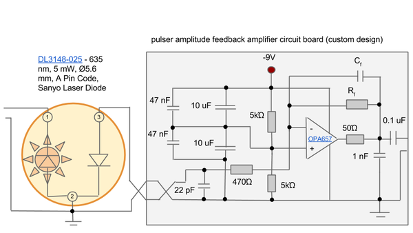
The pulse generator built by Alex Barnes and Jon Kulakofsky produces -10V pulses of duration 1ns fwhm. These pulses are split 90:10 at the output of the pulse generator circuit, and driven out two coaxial cables. The -1V signal matches expectations for a NIM logic signal, and is fed into a discriminator to generate a trigger for the data acquisition. The coaxial cable carrying the -9V pulse is coupled directly from the coax cable conductors to the pins of a laser diode of type DL3148-025 - 635 nm, 5 mW, Ø5.6 mm. The specs for the laser diode are shown at the bottom of this page. The data sheet for the laser diode shows the pin-out for the round 5.6mm package. Pin 2, which is internally shorted to the brass device enclosure, is tied to the braid on the coax, while the coax core conductor is tied to pin 1. Negative pulses provide a forward-biased signal to drive the diode laser. The third pin of the chip is connected to an internal photodiode. If the photodiode is reverse-biased, it generates a current proportional to the intensity of the light in the laser cavity. The photodiode current is said to be 200uA at full laser intensity. It has a stated maximum reverse bias of 30V, but one would guess that it is fully depleted with a reverse bias of only 2-3V. The current from a 1ns pulse would be 200fC. Stretching 200fC over 40ns to have a sufficient pulse width for accurate digitization leaves a pulse maximum of 5uA = 0.25mV at the adc input. Amplification is required if this signal is to be used for pulse height normalization.
Circuit diagram and layout
Figure 1. Circuit diagram of the pulser amplitude feedback amplifier, showing external connections to the 9V power supply, the laser diode package, and the output signal which generates the amplitude feedback pulses.
Figure 2. Layout of the pulser amplitude feedback amplifier circuit board, showing external connections to the 9V power supply, the laser diode package, and the output signal which generates the amplitude feedback pulses. The layout is designed for a standard prototype PCB with traces running in one direction across the board and holes on a 1/10 inch grid. The 9V battery is mounted on the back side of the board. External wires to the laser diode are labeled as 2 and 3. Capacitors are colored purple, resistors are light brown, and wired connections are gray.

