Design and prototyping of SiPM electronics
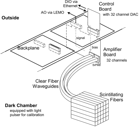
The pages listed here describe the work in electronics undertaken to support Silicon Photomultiplier (SiPM) based readout of the Tagger Microscope for JLab Hall-D and the GlueX experiment in particular. The working design concept for the Tagger's readout involves an array of PCB boards with SiPMs and their amplifiers, summing circuits etc. suspended in a light-tight box out of the plane of incoming electrons. Each of these "amplifier" or "analog" boards are connected across a light-sealing bus board to a "control" or "digital" board. The latter set of boards principally contain bias voltage control circuitry and an architecture that allows Ethernet-based communication with a controlling PC. An added advantage of this two-tier design is the ease with which the tagger can be wired without introducing light leaks: the SiPM signals are passed into a chamber more tolerant of ambient light. (The coaxial cables can then take the SiPM signals off digital boards.) The adjacent diagram outlines this scheme.
Amplifier Boards
Analog Amplifier
The suitability of commercially-available SiPMs have been evaluated with "AMP_0604" amplifier by Photonique.
The following pages provide analysis of this circuit:
- SiPM Amplifier - analog amplifier circuit supplied by for use with the SiPMs.
- MATLAB amplifier in detail - more information regarding the implementation of the MATLAB-based simulation of the amplifier circuit.
A similar amplifier circuit will be designed for every SiPM channel on the board. Those corresponding to a single column will be summed at some stage. Each board, however, will have the capacity for a column of independent channels, since the design of the tagger calls for five such columns in the array.
A separate, second-stage driver will be added to feed the summing circuit (fiber array is read out in groups of 5 channels). The passive components of the circuit are being optimized for tagger use:
Digital Control Boards
Design Tree
- SiPM digital control board - design of the digital PCB for controlling the SiPMs.
- Programming the FPGA
- Programming the Ethernet controller - discussion of the design for the core of the FPGA which handles the complex needs of the FPGA - Ethernet controller chip interface.
- Reset and Initialization - discussion of the design for the reset and initialization part of the core
- Ethernet packets - a detail of the packets we intend to use on our network.
- Programming the DAC - discussion of the design for the DAC.
- Programming the SPI - discussion of the hybrid module that controls both the ADC and the temperature sensor over a single SPI bus. This design incorporates the (now obsolete) predecessor modules:
- Programming the temperature sensor - discussion of the design for the temperature sensor.
- Programming the ADC - discussion of the design for the ADC.
- Programming the Ethernet controller - discussion of the design for the core of the FPGA which handles the complex needs of the FPGA - Ethernet controller chip interface.
- Programming the FPGA
VHDL Overview
- VHDL tutorial - a brief guide to VHDL design with a design example; the introduction and core of the tutorial.
- VHDL: Where to start - section one of the tutorial, focusing on preparing your design for coding.
- VHDL: Enter the code monkey - section two of the tutorial, focusing on outlining the framework of your code.
- VHDL: The real code - section three of the tutorial, focusing on coding the body of your design.
- VHDL: Xilinx ISE - section four of the tutorial, focusing on using the development environment.
To-do list
- Upload ADC module block diagrams
Combine ADC & temperature sensor into single "SPI" module
Complete Ethernet controller moduleRegistersIdlerReaderQuerierProgrammerTransmitterTransceiver, extra debugging quasi-emulators in progressReset moduleCheck all modules for proper async reset supportExecute on startupExecute on commandSoft reset - load and report MAC and location addresses.
Integrate all modules and simulate the device as a wholeDetermine size of FPGA- Design or purchase connector to bus board
- Purchase all components (including EEPROM, RJ-45 female jack, etc)
- Obtain footprints of all chips, connectors, jacks, etc
- PCB layout [in progress]
- Prototype PCB
- Design bus board
- Design analog board
