Characterizing SiPMs
SiPM Performance Requirements
A novel method of low light readout is evaluated here. Traditionally, signals of tens to hundreds of photons are read out by photomultiplier tubes (PMTs), which provide gain of via a cascade of electrons multiplied on collision at each of the device's sequential dynodes. The small cross-section scintillating fibers in the high rate tagger microscope that will operate in Hall-D of Jefferson Lab call for a new and more compact readout. Silicon Photomultipliers (SiPMs) are discussed on the merits of their gain, detection efficiency, speed and noise level.
The tagger microscope consists of many identical and well isolated readout channels, each consisting of a 2 cm scintillating fiber connected to a clear acrylic fiber light guide. A tagging electron travels axially down the length of a scintillating fiber depositing an average of 4 MeV of energy in the fiber, resulting in ~1600 scintillation photons within the forward capture cone of the fiber. Assuming that 80% of these are delivered to the SiPM active surface and a conservative estimate of 15% for the efficiency of the SiPM leads to an estimate of 190 for the average SiPM pixel count per event. Monte Carlo simulations have shown that an efficient detection threshold corresponds to 40% of the average pulse height, or 80 SiPM pixels. This implies a requirement for the dark rate that spontaneous pulses never exceed 80 pixels.
The large photon yield expected at the end of the light guide does not demand unusual detection efficiency on the part of the SiPM. For example, 10% efficiency with the above number of photons still yields a signal of 130 photons. However, given that the scintillator (BCF-20) has a finite decay time (2.7ns) the more photons are produced the more clearly resolved is the leading-edge time of the pulse. (See Tagger Time Resolution)
The device is expected to have a high enough gain (measured in electrons per photon detected) - around 106 in order for such a small light signal to be recorded by conventional electronics. SiPM devices are also susceptible to spurious, thermally excited pixel breakdowns, each showing up as a single photon hit ("dark count"). Very high rates of these single-pixel events may create pileup above the signal threshold. All of the above parameters (detection efficiency, gain and dark rate) depend on applied bias voltage and temperature. Stability of performance within the expected fluctuations of these environmental variables is an important requirement.
Another criterion in SiPM selection is its dynamic range. Although the tagger essentially provides digital information - scintillation detected or not in each energy channel within each beam bucket - sufficient range is necessary to set a threshold above the noise floor and to allow for some degree of gain variation at high rates arising from the finite pixel recovery time.
Bench Test Setup
A fast light source operating in an environment with little background is necessary for the tests described here. The challenge is in preventing light leaks in this chamber despite the need for access ports, patching wires through walls and installing sensor and temperature control modules that must interface with the outside.
A dark chamber was constructed to create this controlled environment. Please refer to the more detailed page on its construction, test and calibration.
SiPM Measurements
Analysis Approach
The first remarkable feature of the the SiPM statistics is the presence of discrete peaks in the histogram of charge collected in the SiPM. The SiPM pulse charge is computed as the SiPM signal integral (Vs) divided by the Gaintrans-impedance (V/A) of the preamplifier. This allows us to determine the charge collected per activated pixel (per detected photon) and therefore gives the gain of the device. This is the "self-calibration" referred to above.
The general analysis procedure was to
- histogram the collected set of function integrals;
- get the pedestal: the first peak corresponds to events with no photon hits, so it defines zero charge collected;
- calculate the gain and rescale the histogram to units of detected photons
Since each peak in the histogram shown in the figure at the right is expressed in units of photon count, the mean is the average number of detected photons per pulse. After subtracting away the contribution from the dark counts (described below), the efficiency of the SiPM can be calculated by comparing this average yield to that found by the HPD.
This procedure was repeated with the LED and/or SiPM covered to measure the dark rate. Depending on which distribution showed the photon peaks more distinctly, either the illuminated or dark datasets were used for the gain calculation and pedestal calculation. Either way, a mean was extracted from the dark distribution to calculate the dark rate and to subtract the average dark pixel count measured from the average pixel count measured while illuminated.
Efficiency calculated in the manner described is compared to the expected efficiency. Integrating the HPD response function in frequency space weighted by the LED emission spectrum yields the mean detection efficiency of the HPD for that light source. The same exercise was carried out using the photon detection efficiency function supplied by the SiPM manufacturer, and compared with the measured efficiency as a check that we had obtained the expected SiPM performance.
Summary of Basic Characteristics and Comparison of SiPMs
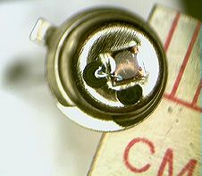
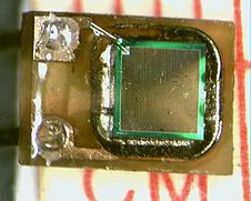
Below is the summary of results obtained from these measurements performed on the two SiPMs acquired from Photonique.
| Device | Gain | PDE (yellow) | Dark Rate | |||
|---|---|---|---|---|---|---|
| Nom. | Meas. | Nom. | Meas. | Nom. | Meas. | |
| SSPM-050701GR-TO18 [4] | 0.8×10⁶ | 1.1×10⁶ | 29% | 30±2% | 10 MHz | 9.8 MHz |
| SSPM-0606BG4-PCB [5] | 1.5×10⁵ | 2.5×10⁵ | 27% | 22±2% | 15 MHz | 8.9 MHz |
Detailed Characterization
Since the SiPM performance is sensitive to the bias voltage applied and the ambient temperature, a measurement of SiPM properties as functions of bias voltage (Vb) and temperature (T) was performed on the SSPM-06. By this point, the SSPM-06 was judged to be a better sensor for the tagger microscope, owing to higher sensitivity in the blue-green range and better active area match to the fiber cross-section. Higher photon detection efficiency is not required for the sake of pulse-height resolution, but it is important in that it improves the time resolution because of the intrinsic scintillation decay time of 2.7 ns in the fiber.
The range of interest for these operating variables were:
- Vb: from 0.5 V below to 0.5 V above the operating range, yielding a range of interest: 19-21 V
- T: 3°C (to avoid accumulating frost) up to 35°C
Histogram Fitting Method
It was found that the individual photon peaks were very indistinct at bias voltages below 20 V and also at temperatures above 20°C. This merging of the peaks is explained by the reduction in pixel gain that occurs for lower bias voltages and higher temperatures, while the electronic noise from the preamplifier remains relatively constant. The solution to this was to abandon the manual location of pedestals, peak spacing etc. Instead, a parametrized model was created by Prof. Richard Jones based on which fitting of the histograms was performed. It has the form:
where,
| where is a gain factor equaling the distance between peaks in Vs. is therefore a unit normalized to pixel counts and zeroed accordingly. | ||
| is the real integral value (in Vs) and is the pedestal offset (location of first peak). | ||
| is the pixel count and Poisson average pixel count | ||
| are multi-Poisson factors that take into account Poisson distributions of secondary pixel counts per each real hit from the set of p hits. | ||
| are random noise parameters. |
are the fit parameters. Note the absence of a vertical scale parameter. The vertical scale depends on the number of samples collected, whereas the equation in this model is normalized. Rescaling works as follows:
If , where is a vertical scaling parameter and since ,
implies that Tg is the number of events collected times the bin width (in Vs).
Now, with this powerful instrument at hand used with a fitter in Paw, the histograms collected as function of T and Vb were analyzed. It turned out that even histograms with nearly indistinguishable peaks yielded a reasonable fit to this model.
Results for SSPM06
Below is the analyzed data on dark rate, gain and photon detection efficiency (PDE) as function of T and Vb. An attempt was also made at mapping the rate of secondaries (multi-Poisson parameter) as a function of these variables but the small trends perceived in the data were within the parameter's error bars.
Results for Hamamatsu 400 pixel MPPC
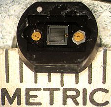
Data were collected with the 1mm x 1mm Hamamatsu MPPC using a similar procedure as was used for the Photonique SiPM studies reported above. The integration window was 250 ns wide, and contained all of the positive side of the signal and about 15% of the negative undershoot tail from the differential-coupled output. The data below were taken with a pulse amplitude giving approximately 1pe per pulse, and with the pulser covered to measure the dark rate (last figure). Each run contains about 15000 samples.
 |

|
 |

|
| Pulse height (V-s) spectrum at fixed pulser intensity and temperature 25°C, and increasing bias voltage Vb = 69.5V (upper left), 70.0V (upper right), 70.2V (lower left), and 71.0V (lower right). | |

|
Pulse height (V-s) spectrum with zero pulser intensity and temperature 25°C, and bias voltage Vb = 70.0V. |
The black histograms in the plots are the data and the red curves are the best fit to the data using the multi-Poisson model described in a preceeding section, with two modifications.
- The Gaussian smearing of the individual pixel pulse-height distribution was replaced with the following function that has an asymmetric tail.
| = | ||
- This function is normalized to unity and is described by parameters:
- = inverse length of left-side tail
- = fraction of peak integral in left-side tail
- = sigma of Gaussian right-side tail =
- The mean cross-talk parameter, formerly pμ in the treatment described above, has been replaced with p2μ.
Without the second change above, the fit to the data is significantly worse. It might be explained by the tendency of cross-talk to bunch up because of self-coupling feedback. A simpler explanation might be that it takes into account a natural variation in the light output of the pulser from pulse to pulse. This remains to be investigated. The parameters of the fit function listed in the above plots are listed below.
- Integral of fit function, in rescaled (pe) x-axis units.
- Centroid of zero pe peak, in V-s.
- Gain of readout, in V-s/pe.
- Mean detected photon count (λp)
- Mean cross-talk pixels per detected photon (λs)
- Excess noise per pixel (σ1), in pe
- α parameter of peak shape function, see above
- σ0 parameter of peak shape function, see above
- β parameter of peak shape function, see above
The Fortran source code where the fit function is implemented can be found here.
MPPC measurement to-do list
- Increase LED output and compare spectra
- Collect spectra of signal peaks as a function of window position (to evaluate distribution of after-pulses)
- Look for methods/components to boost data collection rate
Links
- SiPM Vendors
- Tagger Time Resolution estimates
- BCF-20 Scintillating Fiber (catalog) [6]
- Detection spectrum of the HPD photocathode.
- Photo-sensor Test Stand
- Temperature Controller (vendor page) [7]
- Callibration of the temperature controller: a lookup table for the control and monitor voltage.
- Brandan Krueger's pages on the SiPM Amplifier and MATLAB amplifier in detail
- Photonique SA SiPM Specification Sheets: SSPM-05~ [8] and SSPM-06~ [9]
References
- I. Senderovich and R.T. Jones, "Suitability of Silicon Photomultiplier Devices for Readout of a Scintillating Fiber Tagger Hodoscope", GlueX-doc-760 (2007) [10]
- Z. Sadygov (Dubna), Three advanced designs of avalanche micro-pixel photodiodes: their history of development, present status, maximum possibilities and limitations. [11]
- P.Pakhlov (ITEP), SiPM: Development and Applications [12]
Last edited by Igor Senderovich, June 2008


![{\displaystyle f(q)=\sum _{p,s}\left({\frac {e^{-\lambda }\lambda ^{p}}{p!}}\right)\left({\frac {e^{-p\mu }(p\mu )^{s}}{s!}}\right)\left({\frac {\exp \left(-{\frac {1}{2}}\;{\frac {\left[q-(p+s)\right]^{2}}{\sigma _{0}^{2}+(p+s)\sigma _{1}^{2}}}\right)}{{\sqrt {2\pi }}\left[\sigma _{0}^{2}+(p+s)\sigma _{1}^{2}\right]^{\frac {1}{2}}}}\right)}](https://wikimedia.org/api/rest_v1/media/math/render/svg/980fab6a26e384febe782626eef9cba3abb67852)


![{\displaystyle (1-\beta ){\frac {\alpha }{2}}\,e^{\alpha x+{\frac {\alpha ^{2}\sigma ^{2}}{2}}}\left[1-Erf({\frac {x+\alpha \sigma ^{2}}{{\sqrt {2}}\sigma }})\right]}](https://wikimedia.org/api/rest_v1/media/math/render/svg/7e90f1171c4021ac21f33ad5d321a3cb3d368512)


