Design and prototyping of SiPM electronics
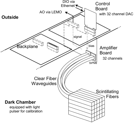
The pages listed here describe the work in electronics undertaken to support Silicon Photomultiplier (SiPM) based readout of the Tagger Microscope for JLab Hall-D and the GlueX experiment in particular. The working design concept for the Tagger's readout involves an array of PCB boards with SiPMs and their amplifiers, summing circuits etc. suspended in a light-tight box out of the plane of incoming electrons. Each of these "amplifier" or "analog" boards are connected across a light-sealing bus board to a "control" or "digital" board. The latter set of boards principally contain bias voltage control circuitry and an architecture that allows Ethernet-based communication with a controlling PC. The merits of this two-tier design is the ease with which the tagger can be wired without introducing light leaks and the separation between digital circuits and analog amplifiers to reduce noise. The adjacent diagram outlines the basic scheme.
Amplifier Boards
SiPM Amplifier
The suitability of commercially-available SiPMs have been evaluated with "AMP_0604" amplifier by Photonique.
The following pages provide analysis of this circuit:
- SiPM Amplifier - analog amplifier circuit supplied by for use with the SiPMs.
- MATLAB amplifier in detail - more information regarding the implementation of the MATLAB-based simulation of the amplifier circuit.
A similar amplifier circuit must be replicated for each SiPM in the tagger microscope. However, microscope readout calls for somewhat different design requirements and operating condition constraints. The following is a brief outline of the demands on the amplifier design:
- adjustable gain, ranging from readout of hundreds of pixels to calibration with single-photon counting
- less than 15% gain variability on transistor beta (hFE) parameter
- summing circuit to pool SiPM signals in groups of 5
- minimized pulse duration
- minimized power consumption
