Digital control board debugging notes
This page contains a list of all currently known problems with the digital control board.
No Power on +1.2V Power Island
Description
The +1.2V island was found to be at 0.0V rather than +1.2V.
Cause
The +5V input (pin 2) on the +1.2V voltage regulator, VR3 (Analog Devices ADP1715), was not connected.
Solution
A dab of solder was used to short pins 1 and 2 on VR3. Pin 1 is an active high chip enable pin, which is permanently tied to +5V.
Other Details and Current Status
This problem was due to an unconnected pin in the original schematics. The schematics have not yet been updated to reflect the solution.
- June 22, 2009: One board has been modified to correct this problem.
SPI Bus Miswired
Description
The SPI bus to the temperature sensor and the ADC is not wired correctly.
Cause
FPGA pin 5 (labelled SPI) is connected to DIN on the ADC, and DOUT of the temperature sensor. FPGA pin 97 (labelled AD7928/DOUT) is connected to DOUT on the ADC. SPI designates that all slave device DOUT traces be connected together. Chip select and HiZ logic are used to prevent devices from fighting over the signal line.
Solution
Pin 5 on the temperature sensor should be connected to pin 18 on the ADC and pin 97 on the FPGA. This can be accomplished by cutting the existing DOUT trace near the temperature sensor and soldering a wire to DOUT on the ADC. In this configuration, pin 5 on the FPGA will become the SPI MOSI (master out, slave in) line, and pin 97 on the FPGA will become the SPI MISO (master in, slave out) line. DIN on the temperature sensor is left tied to ground, since it is not needed.
Other Details and Current Status
This problem was due to errors int he original schematics. The schematics have not yet been updated to reflect the solution.
This modification has been implemented.
Incorrect Oscillator
Description
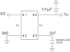
The oscillator used was a standard crystal oscillator, however the FPGA requires an oscillator with a CMOS square wave input.
Solution
The crystal oscillator was replaced with a FOX FXO-HC53 HCMOS oscillator running at 20 Mhz. The output from the oscillator was connected to pin 27 on the FPGA. The load of having both the oscillator and the Ethernet controller connected to the output of the oscillator was to large. The clock input for the Ethernet controller Pin 28 was connected to pin 37 of the FPGA.
Schematic:
Other Details and Current Status
The schematics have not yet been updated to reflect the solution.
This modification has been implemented.
Wrong polarity of Zener Diode on -5V
Zener diode D2 is reversed in the layout. It is correct in the schematics.