Difference between revisions of "Amplifier board debugging notes"
Senderovich (talk | contribs) m |
Senderovich (talk | contribs) |
||
| Line 17: | Line 17: | ||
== Wrong voltage on R<sub>C</sub>/R<sub>D</sub> junction == | == Wrong voltage on R<sub>C</sub>/R<sub>D</sub> junction == | ||
| − | |||
=== Description === | === Description === | ||
| Line 31: | Line 30: | ||
== FET switch compatibility == | == FET switch compatibility == | ||
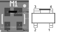
| + | [[Image:AmpBoard_FETorient.png|frame|Quick fix for the package-footprint mismatch of the FET swtich]] | ||
=== Description === | === Description === | ||
The FET switch BF1108 was not available in our market. Only its mirror package variant BF1108R could be procured. | The FET switch BF1108 was not available in our market. Only its mirror package variant BF1108R could be procured. | ||
| Line 36: | Line 36: | ||
=== Solution === | === Solution === | ||
* ''Temporary solution'': The adaptation of the board for the BF1108R is shown in the adjacent figure. The IC is positioned in the shown orientation and its pins (pads) linked as shown. | * ''Temporary solution'': The adaptation of the board for the BF1108R is shown in the adjacent figure. The IC is positioned in the shown orientation and its pins (pads) linked as shown. | ||
| + | * '''modifications of the PCB layout is pending''' | ||
| + | |||
| + | |||
| + | == LEMO receptacle does not fit through holes == | ||
| + | |||
| + | === Description === | ||
| + | The through whole LEMO receptacle does not fit its designated holes. | ||
| + | |||
| + | === Cause === | ||
| + | The pin spacing looks correct, but there does not appear to be sufficient slack in the hole: both pin and hole are specified to be 30mil diameter. Additionally, for the hole size - that specification may only refer to the drill size, not the after-plating diameter. | ||
| + | |||
| + | === Solution === | ||
| + | * The purchases LEMO receptacle pins were filed to fit the holes of the prototype board. | ||
* '''modifications of the PCB layout is pending''' | * '''modifications of the PCB layout is pending''' | ||
Revision as of 16:26, 31 March 2010
This page contains a list of all currently known problems with the amplifier board and the solutions implemented
Improper DC levels from voltage regulators

Description
Incorrect voltage levels on the basis of the transistors representing the input stages for base amplifier and summing circuits.
Cause
The pads for pins Gnd and Vz of the voltage regulators were reversed. The proper assignment of pins is shown in the adjacent figure.
Solution
- the ICs were rotated such that 2 pins (Vref and Gnd) are bonded to their nets. The loose Vz pin was connected via wire to its proper proper net.
- modifications of the PCB layout is pending
Wrong voltage on RC/RD junction
Description
A voltage of 2.75 V was measured on the junction between RC and RD resistors, instead of 2.25
Cause
Resistors RC and RD (2.5 kΩ and 2.0 kΩ respectively) have been reversed. The is an error on the layout: the placement designation and the silk-screen labeling is wrong.
Solution
- The resistors have been swapped.
- modifications of the PCB layout is pending
FET switch compatibility
Description
The FET switch BF1108 was not available in our market. Only its mirror package variant BF1108R could be procured.
Solution
- Temporary solution: The adaptation of the board for the BF1108R is shown in the adjacent figure. The IC is positioned in the shown orientation and its pins (pads) linked as shown.
- modifications of the PCB layout is pending
LEMO receptacle does not fit through holes
Description
The through whole LEMO receptacle does not fit its designated holes.
Cause
The pin spacing looks correct, but there does not appear to be sufficient slack in the hole: both pin and hole are specified to be 30mil diameter. Additionally, for the hole size - that specification may only refer to the drill size, not the after-plating diameter.
Solution
- The purchases LEMO receptacle pins were filed to fit the holes of the prototype board.
- modifications of the PCB layout is pending
