Difference between revisions of "SiPM Amplifier Components"
Senderovich (talk | contribs) m |
Senderovich (talk | contribs) m |
||
| Line 113: | Line 113: | ||
| BJT PNP || NXP (Philips) BFT92W | | BJT PNP || NXP (Philips) BFT92W | ||
|- | |- | ||
| − | | MOSFET || NXP (Philips) BF1108(R)< | + | | MOSFET || NXP (Philips) BF1108(R)<sup>[[#Notes|[1]]]</sup> |
|} | |} | ||
| Line 135: | Line 135: | ||
== Bypass Circuits == | == Bypass Circuits == | ||
| − | The passive components used to bypass high frequency noise to clean up DC levels were picked as follows. The 10 nF capacitor frequently used in the circuit was deemed a good choice - high enough without raising concerns of introducing much inductance. This was also Photonique's choice for bypass capacitors in their prototype amplifier. The resistance on the bases of relevant transistors should be same or lower than that of the bench prototype (200 Ω). 154 Ω is sufficient, leading to a low pass filter with 3 dB point of 100 kHz. Frequencies below this point are well out of the amplifier's band (see [[SiPM Amplifier Signal Analysis]]. | + | The passive components used to bypass high frequency noise to clean up DC levels were picked as follows. The 10 nF capacitor frequently used in the circuit was deemed a good choice - high enough without raising concerns of introducing much inductance. This was also Photonique's choice for bypass capacitors in their prototype amplifier. The resistance on the bases of relevant transistors should be same or lower than that of the bench prototype (200 Ω). 154 Ω is sufficient, leading to a low pass filter with 3 dB point of 100 kHz. Frequencies below this point are well out of the amplifier's band (see [[SiPM Amplifier Signal Analysis]]). |
The bypass circuit for the gate of the MOSFET switch takes more care. Gate resistance forms a voltage divider with resistance on the Source leg. Given the low value of R<sub>d</sub>: 82 Ω, and the MOSFET specification of V<sub>GS</sub> = -4 as the maximum pinch-off value, R<sub>G</sub> of 18 Ω is a good choice. The resulting V<sub>GS</sub> when the controlling voltage is pulled down ground is -4.1 V. | The bypass circuit for the gate of the MOSFET switch takes more care. Gate resistance forms a voltage divider with resistance on the Source leg. Given the low value of R<sub>d</sub>: 82 Ω, and the MOSFET specification of V<sub>GS</sub> = -4 as the maximum pinch-off value, R<sub>G</sub> of 18 Ω is a good choice. The resulting V<sub>GS</sub> when the controlling voltage is pulled down ground is -4.1 V. | ||
| Line 141: | Line 141: | ||
== Notes == | == Notes == | ||
| − | + | ||
| + | # The packaging of BF1108R is a mirror image of that in BF1108. The exact unit is picked depending on the needs of layout. | ||
Revision as of 06:22, 17 March 2009
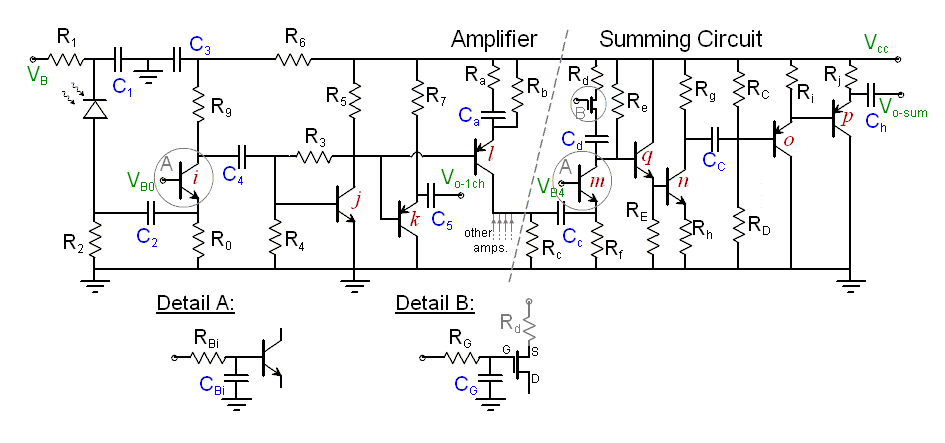
The following presents a more concrete description of components necessary to implement the amplifier design discussed in the SiPM Amplifier Optimization section.
|
|
|
|
| |||||||||||||||||||||||||||||||||||||||||||||||||||||||||||||||||||||||||||||||||||||||||||||||||||||||||||||||||||||||||||||||||||||||||||||||||||||||
Bypass Circuits
The passive components used to bypass high frequency noise to clean up DC levels were picked as follows. The 10 nF capacitor frequently used in the circuit was deemed a good choice - high enough without raising concerns of introducing much inductance. This was also Photonique's choice for bypass capacitors in their prototype amplifier. The resistance on the bases of relevant transistors should be same or lower than that of the bench prototype (200 Ω). 154 Ω is sufficient, leading to a low pass filter with 3 dB point of 100 kHz. Frequencies below this point are well out of the amplifier's band (see SiPM Amplifier Signal Analysis).
The bypass circuit for the gate of the MOSFET switch takes more care. Gate resistance forms a voltage divider with resistance on the Source leg. Given the low value of Rd: 82 Ω, and the MOSFET specification of VGS = -4 as the maximum pinch-off value, RG of 18 Ω is a good choice. The resulting VGS when the controlling voltage is pulled down ground is -4.1 V.
Notes
- The packaging of BF1108R is a mirror image of that in BF1108. The exact unit is picked depending on the needs of layout.
