Difference between revisions of "Digital control board debugging notes"
Senderovich (talk | contribs) m |
(→Incorrect footprint for the Ethernet Jack used: added info about part numbers) |
||
| Line 68: | Line 68: | ||
| − | == | + | == Ethernet jack pinout mismatch == |
| − | |||
| − | |||
| − | |||
| + | The wrong Ethernet jack was attached to the PCB, leading to a pinout mismatch. The part ordered was the Pulse J001'''1'''D21. The correct part is J001'''2'''D21. The correct part was ordered and soldered onto the prototype boards, but this change must be made in the Altium parts list. | ||
= Suggested/Preferred Changes = | = Suggested/Preferred Changes = | ||
* <code>R12</code>, the pull-up resistor for the reset pins (header 2) is unnecessary, as the FPGA pin can be programmed to pull up. | * <code>R12</code>, the pull-up resistor for the reset pins (header 2) is unnecessary, as the FPGA pin can be programmed to pull up. | ||
Revision as of 15:12, 5 November 2009
This page contains a list of all currently known problems with the digital control board.
Problems
No Power on +1.2V Power Island
Description
The +1.2V island was found to be at 0.0V rather than +1.2V.
Cause
The +5V input (pin 2) on the +1.2V voltage regulator, VR3 (Analog Devices ADP1715), was not connected.
Solution
A dab of solder was used to short pins 1 and 2 on VR3. Pin 1 is an active high chip enable pin, which is permanently tied to +5V.
Other Details and Current Status
This problem was due to an unconnected pin in the original schematics. The schematics have not yet been updated to reflect the solution.
- June 22, 2009: One board has been modified to correct this problem.
SPI Bus Miswired
Description
The SPI bus to the temperature sensor and the ADC is not wired correctly.
Cause
FPGA pin 5 (labelled SPI) is connected to DIN on the ADC, and DOUT of the temperature sensor. FPGA pin 97 (labelled AD7928/DOUT) is connected to DOUT on the ADC. SPI designates that all slave device DOUT traces be connected together. Chip select and HiZ logic are used to prevent devices from fighting over the signal line.
Solution
Pin 5 on the temperature sensor should be connected to pin 18 on the ADC and pin 97 on the FPGA. This can be accomplished by cutting the existing DOUT trace near the temperature sensor and soldering a wire to DOUT on the ADC. In this configuration, pin 5 on the FPGA will become the SPI MOSI (master out, slave in) line, and pin 97 on the FPGA will become the SPI MISO (master in, slave out) line. DIN on the temperature sensor is left tied to ground, since it is not needed.
Other Details and Current Status
This problem was due to errors int he original schematics. The schematics have not yet been updated to reflect the solution.
This modification has been implemented.
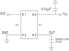
Incorrect Oscillator
Description
The oscillator used was a standard crystal oscillator, however the FPGA requires an oscillator with a CMOS square wave input.
Solution
The crystal oscillator was replaced with a FOX FXO-HC53 HCMOS oscillator running at 20 Mhz. The output from the oscillator was connected to pin 27 on the FPGA. The load of having both the oscillator and the Ethernet controller connected to the output of the oscillator was to large. The clock input for the Ethernet controller Pin 28 was connected to pin 37 of the FPGA.
Schematic:
Other Details and Current Status
The schematics have not yet been updated to reflect the solution.
This modification has been implemented.
Wrong polarity of Zener Diode on -5V
Description
Zener diode D2 is reversed in the layout. It is correct in the schematics.
Solution
The diode was rotated on all the prototyping boards. This indication has not yet been entered into the layout.
Other Details and Current Status
This problem may be related to the overload on the -5V circuitry for of the DAC.
Mismatched JTAG programming header
Description
The connector of the "Xilinx Platform USB II" kit seems to be a reduced size compared to the standard 0.1" spaced pin header with which the board is equipped.
Solution
For the testing stage, the flying lead connector is sufficient to bypass this problem. The layout must be corrected to the matching header (type?). Change entered already?
Ethernet jack pinout mismatch
The wrong Ethernet jack was attached to the PCB, leading to a pinout mismatch. The part ordered was the Pulse J0011D21. The correct part is J0012D21. The correct part was ordered and soldered onto the prototype boards, but this change must be made in the Altium parts list.
Suggested/Preferred Changes
R12, the pull-up resistor for the reset pins (header 2) is unnecessary, as the FPGA pin can be programmed to pull up.