Difference between revisions of "Programming the Ethernet controller"
Senderovich (talk | contribs) m |
Senderovich (talk | contribs) |
||
| (8 intermediate revisions by the same user not shown) | |||
| Line 1: | Line 1: | ||
| − | The modules involved in communication with the Ethernet Controller chip (EC) serve as the core of the FPGA. The | + | The modules involved in communication with the Ethernet Controller chip (EC) serve as the core of the FPGA. The tasks that need to be performed by these modules include |
* executing the complex board reset and address lookup sequence | * executing the complex board reset and address lookup sequence | ||
* polling for new packets and switching execution accordingly | * polling for new packets and switching execution accordingly | ||
| Line 28: | Line 28: | ||
! State !! Module Name !! Description !! Succeeding State | ! State !! Module Name !! Description !! Succeeding State | ||
|- | |- | ||
| − | | align="center" | 000 || [[FPGA_Reset|Reset]]_hard || align="left" |Coordinates the reset and start-up of the EC. || | + | | align="center" | 000 || [[FPGA_Reset|Reset]]_hard || align="left" |Coordinates the reset and start-up of the EC. || 100 |
|- | |- | ||
| − | | align="center" | 001 || [[FPGA_Reset|Reset]]_soft || align="left" | Extends the reset to the PC-requested chips and records PC's MAC for later communication. || | + | | align="center" | 001 || [[FPGA_Reset|Reset]]_soft || align="left" | Extends the reset to the PC-requested chips and records PC's MAC for later communication. || 100 |
|- | |- | ||
| align="center" | 010 || [[FPGA_Idler|Idler]] || align="left" | This is the active module during the FPGA's default idle state. It awaits the "Receive FIFO buffer not empty" interrupt and passes control to the Reader || 011 | | align="center" | 010 || [[FPGA_Idler|Idler]] || align="left" | This is the active module during the FPGA's default idle state. It awaits the "Receive FIFO buffer not empty" interrupt and passes control to the Reader || 011 | ||
| Line 43: | Line 43: | ||
|- | |- | ||
|} | |} | ||
| − | |||
=== State interconnect === | === State interconnect === | ||
As described above, these states form the outline of the functional block diagram. This implementation calls for a central ''state register''. Each block reads the state value in the register and enables itself upon seeing its own value. After completion of its function, a block will write a new value to the state register to enable the next block. With several modules writing to the register, usual precautions must be taken to avoid more than one drivers forcing a line simultaneously. All modules must be designed to go to high impedance on their output lines when they are not active. | As described above, these states form the outline of the functional block diagram. This implementation calls for a central ''state register''. Each block reads the state value in the register and enables itself upon seeing its own value. After completion of its function, a block will write a new value to the state register to enable the next block. With several modules writing to the register, usual precautions must be taken to avoid more than one drivers forcing a line simultaneously. All modules must be designed to go to high impedance on their output lines when they are not active. | ||
| + | |||
| + | |||
| + | == Miscellaneous non-state-based components == | ||
| + | |||
| + | Please refer to the individual design detail pages for: | ||
| + | * [[FPGA_Registers|Registers]] | ||
| + | * [[FPGA_Reusables|Miscellaneous Reusable Components]] | ||
| + | |||
== Interface == | == Interface == | ||
| Line 58: | Line 65: | ||
This communication standard calls for a bridge module that communicates with the EC upon request from other modules. A "[[FPGA_Transceiver|Transceiver]]" was designed for this purpose. It abstracts the communication with the EC as well as the clock frequency difference. This module in fact subdivides the main 20 MHz; clock to generate the "slow" 5 MHz clock for the rest of the FPGA. Please refer to the [[FPGA_Transceiver|detailed page]] on the Transceiver for more information. | This communication standard calls for a bridge module that communicates with the EC upon request from other modules. A "[[FPGA_Transceiver|Transceiver]]" was designed for this purpose. It abstracts the communication with the EC as well as the clock frequency difference. This module in fact subdivides the main 20 MHz; clock to generate the "slow" 5 MHz clock for the rest of the FPGA. Please refer to the [[FPGA_Transceiver|detailed page]] on the Transceiver for more information. | ||
| + | |||
== Combined control flow == | == Combined control flow == | ||
| − | [[Image: | + | [[Image:OperationCourse.png|frame|Operation course between the digital board and the controller PC]] |
| + | Conceptually, the operation course must proceed as outlined in the adjacent figure. The main concern in the tagger control is maintaining a map between board/channel addresses and actual energy bins. For this purpose, the diagrammed two-stage reset plan was devised in the course of which the FPGA learns the PC's MAC address and the PC builds a MAC-Location lookup table. (The "Location" is an 8-byte slot identifier which allows the PC to pinpoint the SiPM channel group.) | ||
| − | + | The internal FPGA operation course that supports this scheme (and the general control board functionality requirements) is outlined below. | |
| − | |||
| − | |||
| − | |||
| − | |||
| + | [[Image:DigBoardScheme.png|center]] | ||
| Line 90: | Line 96: | ||
* Non-state Modules | * Non-state Modules | ||
| − | ** [[FPGA_Transceiver]] | + | ** [[FPGA_Transceiver|Transceiver]] |
| − | ** [[FPGA_Registers]] | + | ** [[FPGA_Interrupt_Catcher|Interrupt Catcher]] |
| + | ** [[FPGA_Registers|Registers]] | ||
* [[Ethernet_packets|Ethernet Packet formatting]] | * [[Ethernet_packets|Ethernet Packet formatting]] | ||
Latest revision as of 06:33, 5 November 2009
The modules involved in communication with the Ethernet Controller chip (EC) serve as the core of the FPGA. The tasks that need to be performed by these modules include
- executing the complex board reset and address lookup sequence
- polling for new packets and switching execution accordingly
- collecting sensor information upon a status report request
- programming the DAC upon a program packet receipt
- building return packets
In our design, the modules involved with packet handling and interfacing with sensor chip controllers are organized by state. A state register specifies the current stage of the process and only the corresponding module is allowed to act during that stage. Aside from defining a process sequence, the state serves as a complex "enable" signal for the modules, ensuring that only one module is driving the communication bus used to query the EC.
Controller
Foreword on Timing
With a controller this complex, the timing of signals must be inspected even more scrupulously than usual. Simultaneity of the rising edge of the "Done" signal and the corresponding output data may not be guaranteed. This is solved by either
- a one-cycle-delayed "Done" signal to ensure that the data lines have been stabilized. (All delays are implemented via the c_delay module which postpones the signal by one cycle via two sequential flip-flops, each shifting by half-cycle).
- coding the target component to read the data lines on the falling edge of the clock during the a "Go" signal.
The latter method turned out to be the dominant one in this design.
The eight states
State-Module organization
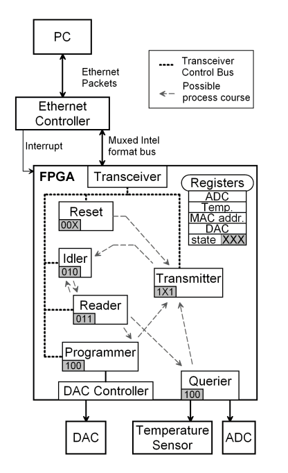
The core of the the FPGA is divided roughly into eight modules enabled by by the 3-bit state value. Below is an index of the states and their corresponding modules. In this discussion of states, 'X' is a binary wild card the values are immediately explained.
| State | Module Name | Description | Succeeding State |
|---|---|---|---|
| 000 | Reset_hard | Coordinates the reset and start-up of the EC. | 100 |
| 001 | Reset_soft | Extends the reset to the PC-requested chips and records PC's MAC for later communication. | 100 |
| 010 | Idler | This is the active module during the FPGA's default idle state. It awaits the "Receive FIFO buffer not empty" interrupt and passes control to the Reader | 011 |
| 011 | [Packet] Reader | Skips the packet header and reads the first two bytes ("location" and "type") of the packet payload. It rejects misdirected or invalid-type bytes. Control is passed according to packet type to Query, Program or Reset Modules | 100, 110, 00X |
| 100 | Querier | Queries the values of the Temperature sensor and ADC, stores them in their respective registers and passes control to the Transmitter for delivery | 101 |
| 110 | [DAC] Programmer | Programs the DAC based on instructions in packet and stores the values in the DAC register. | 111 |
| 1X1 | [Packet] Transmitter | Composes and sends a packet of either 'S' or 'D' type. These correspond respectively to "Status" values reported by the sensor chips (state=101) and current DAC values (state=111) | 010 |
State interconnect
As described above, these states form the outline of the functional block diagram. This implementation calls for a central state register. Each block reads the state value in the register and enables itself upon seeing its own value. After completion of its function, a block will write a new value to the state register to enable the next block. With several modules writing to the register, usual precautions must be taken to avoid more than one drivers forcing a line simultaneously. All modules must be designed to go to high impedance on their output lines when they are not active.
Miscellaneous non-state-based components
Please refer to the individual design detail pages for:
Interface
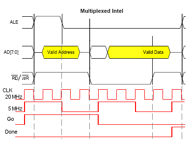
The compact approach to wire and poll the EC is via the Multiplexed Intel bus format. Aside from some use of the interrupt and reset pins, all communication is done via this bus. (The control architecture of the chip uses 8-bit registers selected with 8-bit addresses.) A communication over this bus begins with an pulse on the "ALE" pin, by the fall of which a valid address is expected on the 8-bit inout "AD" bus. After this /RD (/WR) signal falls, executing the read (write) process, and then rises accompanied with valid input from (to) the chip. The adjacent figure illustrates this process along with the approach to timing the conversation taken in this design. Please refer to Section 16.2 in the manual for details on the timing tolerances on this bus.
As shown in the figure, the 20 MHz clock is very convenient for metering this conversation. The communication delay for the FPGA (most of which runs essentially on 5 MHz) turns out to be only two clock cycles.
This communication standard calls for a bridge module that communicates with the EC upon request from other modules. A "Transceiver" was designed for this purpose. It abstracts the communication with the EC as well as the clock frequency difference. This module in fact subdivides the main 20 MHz; clock to generate the "slow" 5 MHz clock for the rest of the FPGA. Please refer to the detailed page on the Transceiver for more information.
Combined control flow
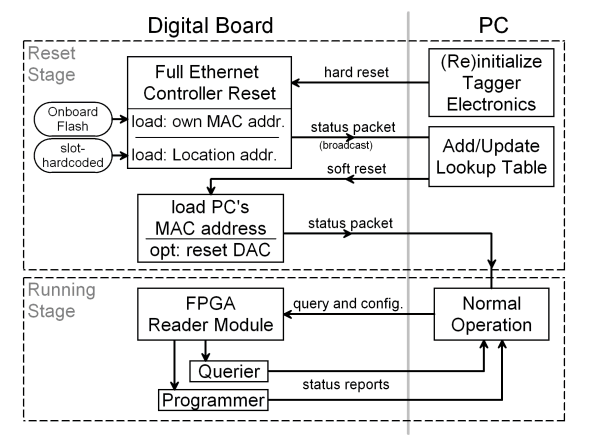
Conceptually, the operation course must proceed as outlined in the adjacent figure. The main concern in the tagger control is maintaining a map between board/channel addresses and actual energy bins. For this purpose, the diagrammed two-stage reset plan was devised in the course of which the FPGA learns the PC's MAC address and the PC builds a MAC-Location lookup table. (The "Location" is an 8-byte slot identifier which allows the PC to pinpoint the SiPM channel group.)
The internal FPGA operation course that supports this scheme (and the general control board functionality requirements) is outlined below.
Emulator
Since the modules described here represent the core of the FPGA, their combined simulation calls for inclusion of all other fringe modules. Essentially the whole FPGA will have to be tested to ensure this scheme for the core is acting properly. The challenge is in the complexity of the stimulus for such simulation: whole packets will need to be sent in and possibly inter-packet Ethernet Controller Chip states tested.
A stripped down emulator for the Ethernet Controller has been written. It is a essentially a set of registers with a Multiplexed Intel bus communication layer and packet file read/write layers. These registers, however, are not passive memory banks but include "events" that are triggered by particular register states. For instance writing to registers designated to make up a receive buffer pointer actually delivers the requested byte from the buffer to the appropriate control register to be available for a subsequent request. A simple interrupt system (stimulated externally by the simulation layer) has also been included.
See Also
- State Modules
- Non-state Modules


