Difference between revisions of "SiPM Amplifier"
Senderovich (talk | contribs) |
|||
| (25 intermediate revisions by 2 users not shown) | |||
| Line 1: | Line 1: | ||
| − | The silicon photomultipliers (SiPM) we are using in our experiment were purchased from [http://www.photonique.ch/ Photonique]. Photonique also supplies analog electronics boards to amplify the signals from the SiPMs. This page discusses the analysis and modeling of the amplifier circuit. | + | The silicon photomultipliers (SiPM) we are using in our experiment were purchased from [http://www.photonique.ch/ Photonique]. Photonique also supplies analog electronics boards to amplify the signals from the SiPMs. This page discusses the analysis and modeling of the amplifier circuit as well as design of the amplifier suitable for the readout of the tagger microscope. |
== The circuit diagram == | == The circuit diagram == | ||
| − | {| align=" | + | The amplifier circuit diagram shown below was developed through combining the diagram supplied by Photonique (lacking component values, and having several extra components) and the physical circuit (having most components labeled). |
| + | |||
| + | The component values are shown below. The capacitors are unlabeled on any diagram, so values are not known for those components. | ||
| + | |||
| + | For information regarding the node voltages and branch currents, see the article on the [[MATLAB amplifier in detail]]. | ||
| + | |||
| + | |||
| + | {| | ||
| + | |[[Image:SSPM Amplifier Circuit Diagram.jpg|thumb|480px|Circuit diagram]] | ||
| + | || | ||
| + | {| align="center" border="1" cellpadding="1" cellspacing="0" style="text-align:center; font-family:times" | ||
|+ '''Component values''' | |+ '''Component values''' | ||
|- | |- | ||
| Line 10: | Line 20: | ||
! colspan="3" style="background:#ffdead; text-align:left" | Resistors | ! colspan="3" style="background:#ffdead; text-align:left" | Resistors | ||
|- | |- | ||
| − | | < | + | | R<sub>1</sub> || 104 || 100kΩ |
|- | |- | ||
| − | | < | + | | R<sub>2</sub> || 103 || 10kΩ |
|- | |- | ||
| − | | < | + | | R<sub>3</sub> || 562 || 5.6kΩ |
|- | |- | ||
| − | | < | + | | R<sub>4</sub> || 202 || 2kΩ |
|- | |- | ||
| − | | < | + | | R<sub>5</sub> || 102 || 1kΩ |
|- | |- | ||
| − | | < | + | | R<sub>6</sub> || 510 || 51Ω |
|- | |- | ||
| − | | < | + | | R<sub>7</sub> || 241 || 240Ω |
|- | |- | ||
! colspan="3" style="background:#ffdead; text-align:left" | Transistors | ! colspan="3" style="background:#ffdead; text-align:left" | Transistors | ||
|- | |- | ||
| − | | < | + | | VT<sub>1</sub> || E2P <small>(1717)</small> || Philips BFS 17A |
|- | |- | ||
| − | | < | + | | VT<sub>2</sub> || W1S <small>(13)</small> || Philips BFT 92 |
| + | |} | ||
|} | |} | ||
| − | |||
| − | + | == MATLAB model == | |
| − | + | :''Main article: [[MATLAB amplifier in detail]]'' | |
| − | : | + | We developed a model for this circuit in MATLAB to simulate its behavior and study various parameters, especially gain as a function of power voltage. The Photonique documentation claims that the power voltage can be varied between four and nine volts in order to tune the gain of the amplifier. The MATLAB model is a linearized system of twenty-four equations, with the voltages and currents on the circuit being the twenty-four unknowns. There are four input parameters: input current (I<sub>in</sub>, in amps), the bias voltage (V<sub>b</sub>, in volts), the power voltage (V<sub>c</sub>, in volts), and the frequency (f, in hertz). The resistor values are mostly the same as the ones given for the above diagram, but some were changed to fit the model to actual data. We also add a load resistor from V<sub>out</sub> to GND, with a value of 50Ω. The transistors are described by a series of parameters from the [http://en.wikipedia.org/wiki/Gummel-Poon_Model Gummel-Poon SPICE model], and we included our best guesses of the capacitor values. |
| − | + | The model itself can be found [http://zeus.phys.uconn.edu/halld/tagger/electronics/design-6-2007/SSPM_amp.zip here]. | |
== Responses of the model == | == Responses of the model == | ||
| − | We ran simulations of the MATLAB model while varying the input parameters to generate data on how the amplifier responds to each input. We used as a baseline test the inputs < | + | We ran simulations of the MATLAB model while varying the input parameters to generate data on how the amplifier responds to each input. We used as a baseline test the inputs V<sub>b</sub> = 20V, V<sub>c</sub> = 5V, f = 100MHz, and I<sub>in</sub> = 1mA, then varied one parameter at a time to generate responses. |
=== Bias voltage === | === Bias voltage === | ||
| − | + | We varied the bias voltage from 0 to 50V. Within this range the output (V<sub>out</sub>) does not vary at all. | |
=== Power voltage === | === Power voltage === | ||
| − | The amplifier's response to varying the power voltage (< | + | The amplifier's response to varying the power voltage (V<sub>c</sub>) from 0 to 10V is shown in the image below. |
| − | [[Image:Amplifier Response to Power. | + | [[Image:Amplifier Response to Power (2007-07-03).png]] |
| − | Note that the vertical axis can be read as either the output voltage (< | + | Note that the vertical axis can be read as either the output voltage (V<sub>out</sub>) in mV or as the transimpedance gain in Ω. |
=== Frequency === | === Frequency === | ||
| − | The amplifier's response to varying the frequency ( | + | The amplifier's response to varying the frequency (f) is shown in the image below. |
| − | [[Image:Amplifier Response to Frequency. | + | [[Image:Amplifier Response to Frequency (2007-07-03).png]] |
| − | Note that the vertical axis can be read as either the output voltage (< | + | Note that the vertical axis can be read as either the output voltage (V<sub>out</sub>) in mV or as the transimpedance gain in Ω. |
=== Input current === | === Input current === | ||
| − | Varying the input current from 0 to 2A results in a clean straight line. | + | Varying the input current from 0 to 2A results in a clean straight line that intersects the origin. Thus we can say that the amplifier has a transimpedance gain (programmable based on input parameters; in particular V<sub>c</sub>) and no DC bias. |
| − | + | ||
| − | Thus we can say that the amplifier has a transimpedance gain (< | + | |
| + | == Limitations of the Model == | ||
| + | |||
| + | One of the principal limitations of this model turned out to be its inability to predict high-frequency behavior. Though the bandwidth inherent in the transistors themselves (4-5 GHz) was not explicitly in the model, the low-pass behavior due to source capacitance and amplifier input impedance should appear in the solutions naturally. It turned out that the more accurate modeling of the SiPM discharge as parallel injection of I<sub>in</sub> ''in parallel'' with the intrinsic SiPM capacitor recovers this behavior. Including this capacitance (labeled ''CS'') and a parallel current injection loop restored the sensitivity to input impedance. This input impedance turned out to be a challenge for achieving faster signals desired in the tagger microscope electronics. This issue is further discussed in a dedicated page:[[SiPM Amplifier Optimization]] | ||
Latest revision as of 21:33, 27 February 2009
The silicon photomultipliers (SiPM) we are using in our experiment were purchased from Photonique. Photonique also supplies analog electronics boards to amplify the signals from the SiPMs. This page discusses the analysis and modeling of the amplifier circuit as well as design of the amplifier suitable for the readout of the tagger microscope.
The circuit diagram
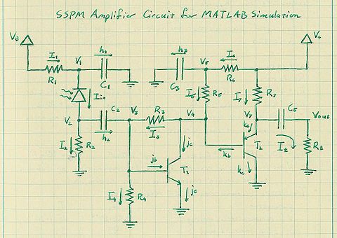
The amplifier circuit diagram shown below was developed through combining the diagram supplied by Photonique (lacking component values, and having several extra components) and the physical circuit (having most components labeled).
The component values are shown below. The capacitors are unlabeled on any diagram, so values are not known for those components.
For information regarding the node voltages and branch currents, see the article on the MATLAB amplifier in detail.
| |||||||||||||||||||||||||||||||||||||
MATLAB model
- Main article: MATLAB amplifier in detail
We developed a model for this circuit in MATLAB to simulate its behavior and study various parameters, especially gain as a function of power voltage. The Photonique documentation claims that the power voltage can be varied between four and nine volts in order to tune the gain of the amplifier. The MATLAB model is a linearized system of twenty-four equations, with the voltages and currents on the circuit being the twenty-four unknowns. There are four input parameters: input current (Iin, in amps), the bias voltage (Vb, in volts), the power voltage (Vc, in volts), and the frequency (f, in hertz). The resistor values are mostly the same as the ones given for the above diagram, but some were changed to fit the model to actual data. We also add a load resistor from Vout to GND, with a value of 50Ω. The transistors are described by a series of parameters from the Gummel-Poon SPICE model, and we included our best guesses of the capacitor values.
The model itself can be found here.
Responses of the model
We ran simulations of the MATLAB model while varying the input parameters to generate data on how the amplifier responds to each input. We used as a baseline test the inputs Vb = 20V, Vc = 5V, f = 100MHz, and Iin = 1mA, then varied one parameter at a time to generate responses.
Bias voltage
We varied the bias voltage from 0 to 50V. Within this range the output (Vout) does not vary at all.
Power voltage
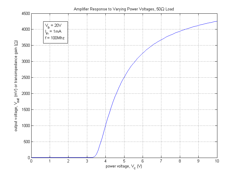
The amplifier's response to varying the power voltage (Vc) from 0 to 10V is shown in the image below.
Note that the vertical axis can be read as either the output voltage (Vout) in mV or as the transimpedance gain in Ω.
Frequency
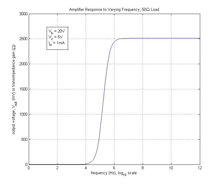
The amplifier's response to varying the frequency (f) is shown in the image below.
Note that the vertical axis can be read as either the output voltage (Vout) in mV or as the transimpedance gain in Ω.
Input current
Varying the input current from 0 to 2A results in a clean straight line that intersects the origin. Thus we can say that the amplifier has a transimpedance gain (programmable based on input parameters; in particular Vc) and no DC bias.
Limitations of the Model
One of the principal limitations of this model turned out to be its inability to predict high-frequency behavior. Though the bandwidth inherent in the transistors themselves (4-5 GHz) was not explicitly in the model, the low-pass behavior due to source capacitance and amplifier input impedance should appear in the solutions naturally. It turned out that the more accurate modeling of the SiPM discharge as parallel injection of Iin in parallel with the intrinsic SiPM capacitor recovers this behavior. Including this capacitance (labeled CS) and a parallel current injection loop restored the sensitivity to input impedance. This input impedance turned out to be a challenge for achieving faster signals desired in the tagger microscope electronics. This issue is further discussed in a dedicated page:SiPM Amplifier Optimization


